

Plasma Etching Focus Ring: An Essential Component in Semiconductor Manufacturing
2025-05-07
In the field of semiconductor manufacturing, precision is paramount. Every process, from wafer fabrication to device assembly, requires meticulous attention to detail. One such crucial process is plasma etching, a technique used to etch fine patterns on semiconductor materials. The Plasma Etching Focus Ring plays a vital role in ensuring the effectiveness and quality of this process. This article explores the function, importance, and key features of the plasma etching focus ring in semiconductor production.
What is Plasma Etching?
Plasma etching is a form of dry etching that uses ionized gases (plasma) to etch intricate patterns onto semiconductor wafers. The process involves generating a plasma field by applying an electric field to a gas, which then ionizes the gas molecules. These charged particles, or ions, react with the surface of the wafer, removing material and creating patterns with incredible precision. Plasma etching is widely used in the fabrication of integrated circuits (ICs) and microelectromechanical systems (MEMS).
What is a Plasma Etching Focus Ring?
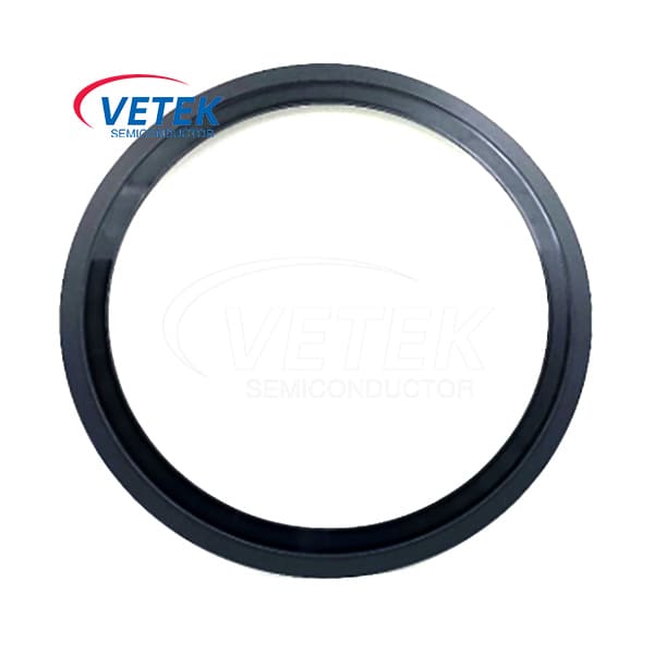
A Plasma Etching Focus Ring is a critical component used in the plasma etching process. Positioned at the top of the etching chamber, the focus ring helps to shape the plasma field, ensuring uniformity across the surface of the wafer. It is typically made of a durable material that can withstand the harsh conditions inside the etching chamber, such as high temperatures, ion bombardment, and chemical reactions.
The focus ring's primary function is to control the plasma's intensity and uniformity, directing the etching process to ensure that the wafer receives consistent exposure to the plasma. This helps to maintain the precision needed for the delicate patterns that are etched onto the semiconductor materials.
Key Functions of the Plasma Etching Focus Ring
1. Plasma Uniformity Control
One of the key roles of the plasma etching focus ring is to ensure uniform plasma distribution across the surface of the wafer. It helps to focus the plasma ions evenly over the wafer, preventing areas of over-etching or under-etching. This is especially important for semiconductor applications, where uniform etching is crucial for the integrity of the device's electrical characteristics.
2. Enhanced Etching Precision
The focus ring aids in controlling the etching depth and pattern fidelity by minimizing unwanted variations in the plasma field. In high-precision industries such as semiconductor manufacturing, even a small deviation in etching can lead to defects that compromise the functionality of the device. The focus ring ensures that the etching process is as precise as possible.
3. Protection of Chamber Components
The plasma etching process generates high-energy ions and reactive species, which can damage sensitive parts of the etching chamber. The focus ring helps to protect the chamber’s components by acting as a shield. It absorbs or diverts some of the energy from the plasma, preventing the erosion of critical parts of the equipment and extending the chamber's lifespan.
4. Heat Distribution
Plasma etching is an energy-intensive process that generates significant amounts of heat. The focus ring helps to dissipate some of this heat, maintaining a more stable temperature within the etching chamber. Proper heat distribution is essential to prevent overheating, which can affect the consistency and accuracy of the etching process.
Materials Used in Plasma Etching Focus Rings
Plasma etching focus rings are constructed from materials that can withstand the harsh conditions of the etching chamber. Common materials include:
Ceramic Materials: Ceramics are often chosen due to their ability to withstand high temperatures and resist the corrosive effects of the plasma. Materials such as alumina or silicon carbide are commonly used for focus rings.
Quartz: Quartz is another popular material because of its excellent resistance to high-energy ion bombardment. It also has high thermal stability, which is crucial during the etching process.
Graphite: In some cases, graphite is used for focus rings due to its high-temperature tolerance and resistance to erosion in the plasma environment.
The choice of material depends on the specific requirements of the etching process, such as the type of plasma used, the temperature, and the specific etching application.
Importance of Plasma Etching Focus Rings in Semiconductor Manufacturing
In semiconductor manufacturing, precision and consistency are vital. A slight variation in the etching process can lead to the failure of entire batches of wafers, resulting in significant financial losses. The plasma etching focus ring plays an essential role in maintaining these precise conditions.
1. Minimizing Defects
In the production of semiconductors, even the smallest defect can cause a chip to malfunction. The focus ring ensures that the plasma etching process is uniform across the wafer, reducing the likelihood of defects such as uneven etching or pattern distortion.
2. Maximizing Yield
Yield, the ratio of functional chips produced to the total number of chips processed, is a critical metric in semiconductor production. A focus ring ensures that the etching process is as accurate and uniform as possible, which directly contributes to a higher yield. High yields are essential for cost efficiency and competitiveness in the semiconductor market.
3. Cost Efficiency
While focus rings might seem like a small component in the overall manufacturing process, their role in ensuring precise etching and protecting the etching chamber from damage ultimately contributes to the overall efficiency of the process. By extending the life of chamber components and minimizing defects, the use of focus rings helps to reduce overall production costs.
4. Improving Device Performance
Since plasma etching is used to create intricate patterns on semiconductor wafers, the accuracy of the process is crucial for the final device's performance. The focus ring helps achieve the desired patterning and etching depth, ensuring the devices perform as intended in their respective applications, from smartphones to medical devices and beyond.
Conclusion
The Plasma Etching Focus Ring is an essential component in the plasma etching process, playing a critical role in achieving precision and uniformity in semiconductor manufacturing. By ensuring an even distribution of plasma, enhancing etching precision, and protecting chamber components, focus rings contribute significantly to the efficiency, accuracy, and reliability of the etching process. As the demand for smaller, faster, and more efficient semiconductor devices grows, the role of components like the plasma etching focus ring will continue to be a key factor in driving innovation and improving manufacturing outcomes in the electronics industry.